Fu Jia Ga Ye, a prominent player in the semiconductor materials industry, has announced a significant technological advancement in the field of gallium oxide (Ga2O3) crystal growth. The company has successfully cultivated 6-inch gallium oxide single crystal ingots with a thickness exceeding 70mm, utilizing their proprietary Vertical Bridgman (VB) method. This achievement marks a crucial step forward in the mass production of this promising wide-bandgap semiconductor material.
Key Technological Advancements
The successful growth of thicker ingots is a critical indicator of the maturity and industrial scalability of single crystal growth technology. A greater ingot thickness directly translates to more substrate wafers being cut from a single crystal, thereby reducing the cost per wafer – a vital factor for widespread adoption in the industry.
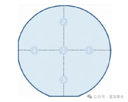
Independent verification from the Pinghu Laboratory confirmed the excellent crystalline quality of the ingots through High-Resolution X-ray Diffraction (HRXRD) testing. The average Full Width at Half Maximum (FWHM) across five measurement points was recorded at 38.71 arcseconds, consistently below the 50 arcsecond threshold, indicating a high degree of crystal perfection.
Furthermore, the National Institute of Metrology, China, conducted rigorous electrical performance testing on the 6-inch gallium oxide substrates. The results demonstrated an average resistivity of 16.4 mΩ·cm with a uniformity of 6.8%. These electrical properties meet the stringent requirements for substrates needed in the silicon carbide (SiC) industry, highlighting the potential of Ga2O3 to serve as a complementary or alternative material.
The specific dimensions of the ingot were confirmed by the National Institute of Metrology, China, with an average thickness of 70.58 mm and a variation of only 0.12 mm. This thickness significantly surpasses that of mainstream silicon carbide ingots, which typically range from 20-50 mm in height.
Significance for the Semiconductor Industry
Gallium oxide is a wide-bandgap semiconductor material with exceptional properties, including high breakdown voltage and low on-resistance, making it highly suitable for power electronics applications. Its potential to outperform silicon carbide (SiC) and gallium nitride (GaN) in certain high-voltage scenarios has garnered significant attention from researchers and manufacturers worldwide.
The ability to produce larger and thicker Ga2O3 ingots is paramount for driving down manufacturing costs and enabling the commercial viability of Ga2O3-based devices. This breakthrough by Fu Jia Ga Ye directly addresses these challenges, paving the way for Ga2O3 to compete more effectively in the power semiconductor market, which is currently dominated by SiC and GaN technologies.
Upcoming Industry Showcase
Fu Jia Ga Ye plans to showcase its latest advancements at the 20th National Crystal Growth and Materials Academic Conference. The conference, scheduled to take place from August 22-25, 2026, in Jinan, Shandong Province, will feature an exhibition where Fu Jia Ga Ye will present a comprehensive range of 2-inch to 8-inch gallium oxide substrates and epitaxy products. Attendees will have the opportunity to view samples with various crystal orientations, including (100), (010), (001), and (011) plane orientations.
This upcoming exhibition provides a platform for Fu Jia Ga Ye to engage with industry peers, potential customers, and researchers, further solidifying its position as a leader in the development and production of advanced gallium oxide materials.