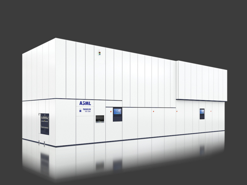
In the relentless pursuit of smaller and more powerful semiconductors, advanced lithography techniques are paramount. ASML, a leading manufacturer of chipmaking equipment, and its optical systems partner ZEISS, have shed light on the future of extreme ultraviolet (EUV) lithography. In a recent publication, they detailed the primary challenge facing the next generation of ‘Hyper NA EUV’ lithography machines: a significantly reduced usable depth of field.
The Evolution of EUV Lithography
The journey towards ever-denser circuitry involves pushing the boundaries of light and optics. Current High NA EUV lithography systems, which are already cutting-edge, utilize a numerical aperture (NA) to define their resolution capabilities. The upcoming Hyper NA EUV machines are poised to push this NA to at least 0.75, a considerable leap from current standards.
This advancement is seen as a logical progression, maintaining the 13.5nm wavelength of EUV light while increasing the NA. The potential payoff is substantial: the ability to achieve an optical resolution of 5nm ‘half-pitch,’ a key metric for transistor density. This technology is anticipated to become available within the next decade, around 2034.
Key Technical Hurdles Ahead
While the optical system for a 0.75 NA Hyper NA EUV machine is expected to be only slightly larger than existing High NA EUV setups, ensuring compatibility with current cleanroom infrastructure, the core challenge lies in managing the diminished usable depth of field. This limitation necessitates a multi-faceted approach to process control:
- Thinner Photoresists: To maintain focus across the wafer, the light-sensitive material (photoresist) used in the lithography process will need to be thinner.
- Enhanced Focus Control: Scanning equipment will require more sophisticated and precise focus control mechanisms.
- Wafer Flatness: Achieving and maintaining exceptional wafer flatness becomes even more critical to ensure uniform exposure.
- Process Control Improvements: Overall process control methodologies will need significant refinement to compensate for the tighter tolerances.
The article suggests that extending the NA further, for instance to 0.85 NA, would lead to a substantial increase in system size, potentially diminishing its practicality and market appeal. Therefore, the focus remains on optimizing the 0.75 NA system.
Compatibility and Reusability
A significant advantage highlighted by ASML and ZEISS is the potential for compatibility with existing infrastructure and components. Through optical and mechanical refinements, it is anticipated that the mask foundation used in current EUV systems could be largely reused with Hyper NA EUV machines. Furthermore, the light source systems are also expected to be compatible, reducing the overall investment and development time for foundries looking to adopt this next-generation technology.
This collaborative effort between ASML and ZEISS underscores the complex engineering and innovation required to drive semiconductor manufacturing forward. The successful implementation of Hyper NA EUV lithography will be a testament to overcoming these intricate technical challenges, paving the way for the next era of integrated circuits.