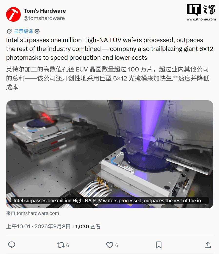
In a significant technological leap, Intel has announced it has processed over one million 300mm wafers using High-Numerical Aperture Extreme Ultraviolet (High-NA EUV) lithography equipment. This remarkable achievement comes in less than two and a half years since the assembly of their first High-NA EUV machine, underscoring Intel’s rapid adoption and mastery of this cutting-edge technology.
Dominating the High-NA EUV Landscape
Intel’s current arsenal includes two ASML Twinscan EXE:5000 prototype machines and at least one EXE:5200B production model. The company’s progress has been swift, processing approximately 30,000 wafers by February 2025 and surpassing the one million mark by September 2026. This pace is so exceptional that Intel’s wafer processing volume using High-NA EUV now exceeds the combined total of all other industry users.
Data revealed by ASML in their first-quarter 2026 earnings report showed that the global cumulative wafer processing for all High-NA EUV systems at that time was just over 500,000, with an uptime exceeding 80%. This starkly contrasts with Intel’s individual output, solidifying its position as the leader in this advanced manufacturing domain.
Enabling Next-Generation Processors
Intel has already leveraged High-NA EUV to validate its Intel 18A process node. This advanced technology is currently in use for the production of the upcoming Panther Lake series of Core Ultra processors. Earlier this year, ASML recognized Intel as the world’s first company to achieve large-scale shipments of logic chips manufactured with High-NA EUV.
Furthermore, specific process layers within Intel 18A have completed High-NA EUV dual certification, with yields matching the current NXE EUV platform. This indicates a high level of maturity and reliability for the technology in mass production.
Addressing Future Challenges: The Reticle Size Dilemma
Despite these impressive strides, High-NA EUV faces a significant hurdle: the limitation imposed by current reticle (mask) dimensions. To overcome this, Intel is spearheading an industry-wide initiative to transition to larger 6×12 inch reticles. This larger format would enable a full 26x33mm field of view in a single exposure, a crucial step for future chip designs.
However, this proposed shift necessitates substantial changes across the entire reticle ecosystem. This includes modifications to blank substrates, deposition, etch, inspection, metrology, cleaning, pellicles, mask writing equipment, and handling systems. The High-NA EUV machines themselves would also require adaptation or redesign to accommodate the larger reticles.
It’s worth noting that ASML’s roadmap indicates that High-NA EUV systems introduced around and after 2033 will continue to be based on the 6×6 inch reticle and stitching approach. Neither ASML nor Intel has yet confirmed whether existing or planned High-NA EUV lithography machines can be retrofitted to support the proposed 6×12 inch reticles. This ongoing discussion highlights the complex collaborative efforts required to push the boundaries of semiconductor manufacturing.