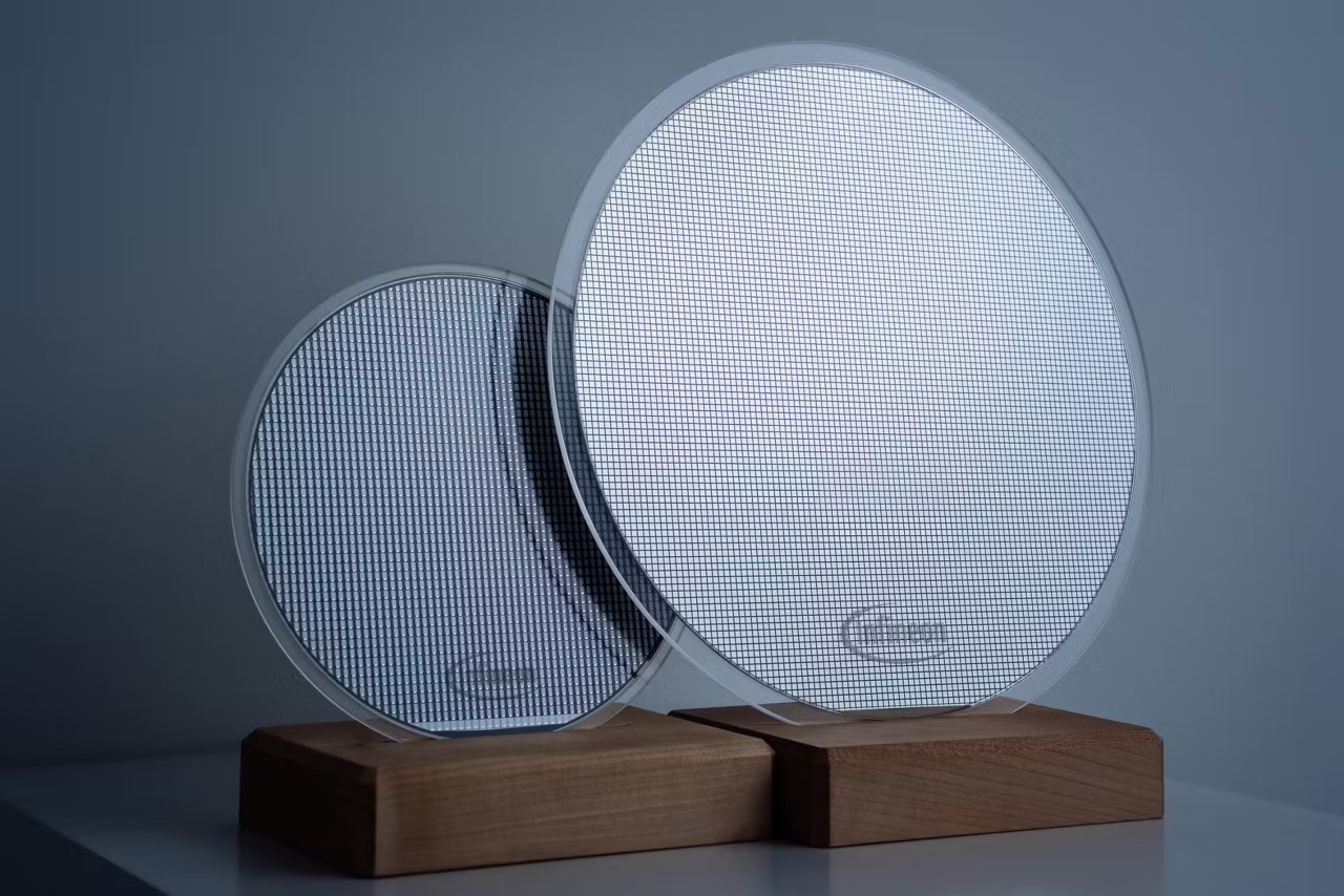
Infineon Technologies has achieved a significant milestone in semiconductor manufacturing, announcing the successful processing of 300mm (12-inch) silicon carbide (SiC) wafers into power semiconductor devices within a full-scale semiconductor fabrication plant environment. This groundbreaking achievement marks a first for the industry and was accomplished using existing silicon (Si) semiconductor manufacturing equipment at Infineon’s Villach fab in Austria.
Paving the Way for Larger SiC Wafers
The successful production demonstrates the commercial viability of large-diameter SiC wafers. This advancement is crucial for the next generation of power electronics, which demand higher performance, efficiency, and reliability. SiC technology is key to enabling advancements in electric vehicles, renewable energy systems, and industrial power supplies.
Infineon plans to work closely with its customers and partners to define the roadmap for 12-inch SiC technology and its mass production timeline. In parallel, the company continues to advance its existing 200mm SiC manufacturing roadmap, ensuring a steady supply of SiC devices for current market needs.
Innovations in SiC Manufacturing
Further bolstering its SiC manufacturing capabilities, Infineon has also validated its ‘cool slicing’ technology on 12-inch SiC wafers at its Dresden facility in Germany. This innovative process enhances the efficiency of the ingot-to-wafer production process. By reducing material loss during wafer slicing, cool slicing contributes to improved cost-effectiveness and sustainability in SiC wafer production.
The transition to larger wafer sizes, from 200mm to 300mm, is a standard progression in semiconductor manufacturing. It typically leads to a significant increase in the number of devices that can be produced per wafer, thereby driving down costs and improving manufacturing efficiency. For SiC, which is generally more expensive to process than traditional silicon, this scaling is particularly important for widespread adoption.
Future Outlook for SiC Technology
Infineon’s leadership in developing and implementing 300mm SiC wafer processing underscores its commitment to innovation and its strategic position in the growing SiC market. The company’s ability to leverage existing manufacturing infrastructure for this new technology demonstrates a forward-thinking approach to scaling production.
The benefits of SiC power devices include lower energy losses, higher operating temperatures, and greater power density compared to traditional silicon-based devices. These advantages make them ideal for demanding applications such as electric vehicle charging infrastructure, onboard chargers, and high-voltage power grids.
As the demand for more efficient and sustainable energy solutions continues to rise, Infineon’s advancements in SiC manufacturing are poised to play a critical role in shaping the future of power electronics.