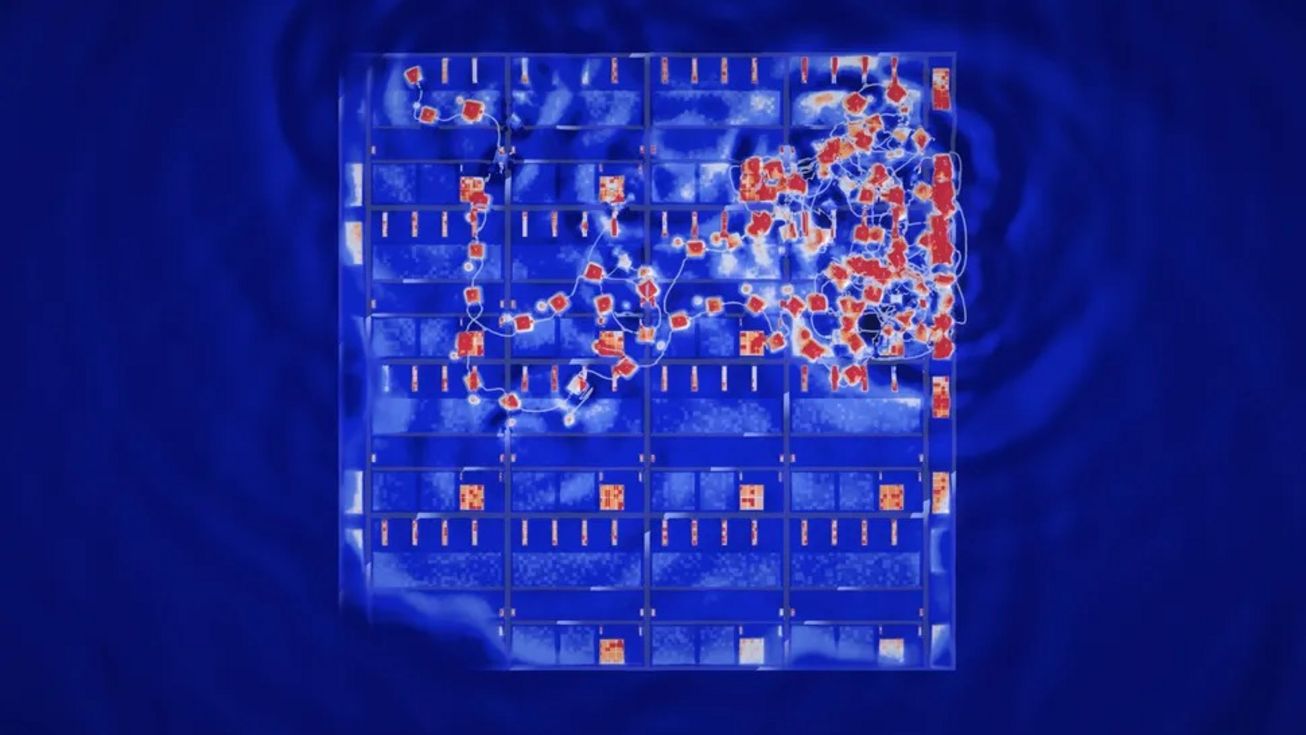
The Frostbite CPU architecture from Architect Labs, a Silicon Valley startup, promises a breakthrough in processor efficiency. According to recent tests, this AI-designed CPU cluster delivers up to 4.59 times the performance per watt compared to a similar-sized, silicon-verified traditional CPU core.
This innovative CPU, revealed in a research blog, was developed without relying on conventional architectural models. Instead, AI systems autonomously designed and verified the chip’s instruction set and structure, aiming to overcome inherent limitations of traditional CPU designs.
AI-Driven Design and Novel Architecture
The Frostbite processor is composed of multiple identical small compute units called Tiles, interconnected by an on-chip network and equipped with small local memories. Unlike typical CPUs that rely on complex hardware to manage instruction dependencies and cache coherence, Frostbite uses a “Multithreading for Free” approach where programs explicitly expose parallel work, eliminating traditional threading and locks.
The current test cluster includes 4 Tiles and 4 L3 cache nodes, but the full design scales up to 16 Tiles. Initial synthesis achieved clock speeds up to 800MHz, later settled at 500MHz in physical design stages. Performance evaluations, based on simulations with a 7nm process design, point to a performance advantage in energy efficiency ranging widely by workload, with a peak improvement of over 23x in conv2d operations.
Advanced AI Tools for Hardware Validation
From the outset, Architect Labs’ AI agents crafted detailed design documents, moving from natural language descriptions to a formal hardware specification language called ASL, enabling machine-verified correctness. Before hardware design commenced, an AI-created software model named Arcmodel was developed to simulate chip behavior 200 times faster than RTL simulation, facilitating rapid iteration.
Throughout the development, the AI evaluated 58 optimization strategies, adopting 37 that passed rigorous specification, simulation, and power tests. The processor also exhibited an unexpected beneficial behavior dubbed “work stealing,” where idle Tiles dynamically acquire tasks from neighbors to maintain efficiency.
Energy distribution in Frostbite differs significantly from traditional CPUs. Instruction fetch and decode consume only 6% of its power versus 27% in conventional designs, although on-chip network and scheduler overhead add 26%. The architecture drastically reduces latency and power-hungry hardware needed for instruction dependency detection and cache coherence.
While these results are promising, Frostbite remains a simulated design without fabricated silicon. Architect Labs plans further performance evaluations, broader benchmark testing, and eventual open release of RTL code and the instruction set. The company also intends to launch an online FPGA platform for public experimentation and develop an initial operating system.
Alongside Architect Labs, other startups like Tendrils Compute are exploring massively parallel processor designs and new programming languages to harness them, indicating growing momentum in AI-assisted chip innovation.