The escalating demand for advanced chips and the increasing complexity of their manufacturing processes necessitate unparalleled precision from engineers, where errors are simply not an option. Traditional analysis methods and physical experiments on production lines are time-consuming and costly, and incorrect decisions regarding yield or process quality have tangible consequences.
Artificial Intelligence (AI) is revolutionizing semiconductor manufacturing, significantly enhancing engineers’ capabilities and accelerating their workflows. The use of accelerated computing drastically cuts down simulation times, allowing engineers to evaluate more alternatives before physical testing. Physics-informed AI helps predict process behavior without the need for full-scale modeling. AI agents automate sequences of engineering tasks that previously consumed hours. Furthermore, digital twins provide teams with the ability to test changes in a virtual environment before implementing them in actual production.
The combination of these capabilities is shaping the concept of an “AI-defined fab” – a semiconductor manufacturing environment where AI assists in optimizing processes, detecting issues earlier, and making better decisions throughout a chip’s entire lifecycle. Engineers, while retaining their crucial role in directive management and expertise-driven decision-making, spend less time waiting for results.
Reduced Simulation Cycles Expand Research Capabilities
Accelerated computing doesn’t just speed up individual calculations; it increases the number of alternatives engineers can test before committing to physical trials. Multi-physics simulations model the interplay between physical effects such as heat transfer, electrical behavior, and mechanical stresses. Thanks to the NVIDIA cuDSS library, simulation software provider COMSOL is accelerating such simulations for semiconductor manufacturing by up to 10 times. This empowers engineers to optimize equipment and processes, compare alternatives, and determine which changes are worth pursuing physically.
Applied Materials and NVIDIA are collaborating to accelerate material discovery at the atomic level and process development. The integration of NVIDIA cuDSS enables the Applied Ginestra platform to operate up to 10 times faster compared to approaches relying solely on central processing units (CPUs). With NVIDIA PhysicsNeMo, Applied’s ACE+ multi-physics platform delivers up to a 35x acceleration for topography simulations.
In some instances, acceleration doesn’t merely reduce calculation time; it makes them feasible. Computational lithography, which dictates how circuits are patterned onto silicon, involves calculations far too complex for CPUs to handle at a production scale. Siemens is integrating NVIDIA cuLitho into its Calibre software, achieving up to a 17x acceleration on key simulation workloads. This expands engineers’ ability to verify parameters before wafer printing.
Consequently, accelerated calculations are instrumental in enabling researchers to explore material behaviors and reaction pathways critical for next-generation semiconductor manufacturing processes.
Predicting Process Behavior Without Full-Scale Simulations
Beyond speeding up simulations, AI trained on physical models can predict the behavior of materials and processes without the need to run a full simulation every time. This is particularly noticeable in complex calculations that remain costly even on accelerated hardware.
One such example is plasma, a charged gas used in semiconductor etching processes. Modeling plasma requires solving equations that account for the interaction of electrical, chemical, and thermal phenomena, making repeated simulations expensive. Lam Research has demonstrated that NVIDIA PhysicsNeMo framework can predict plasma behavior in milliseconds, whereas a full simulation takes days. This provides engineers with a faster method to explore process conditions without re-running the complete model.
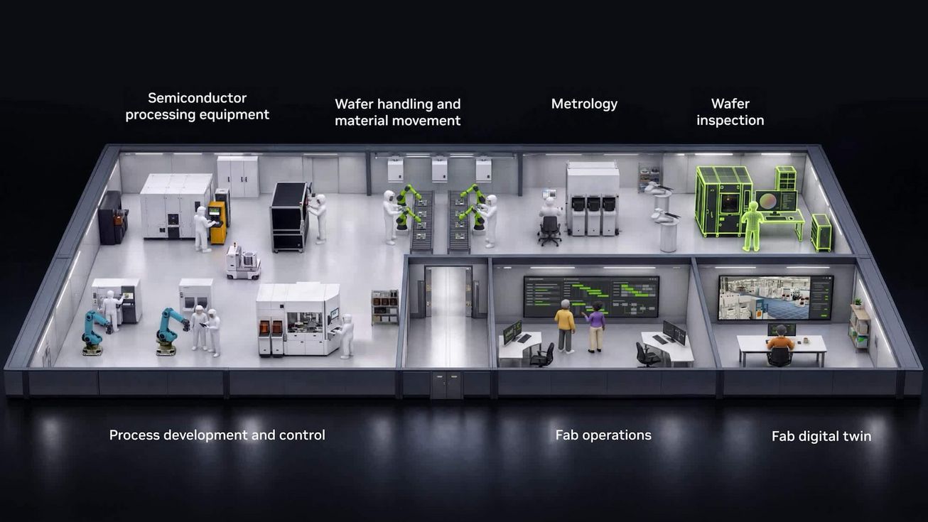
Applied Materials is leveraging digital twins built on NVIDIA Omniverse libraries to simulate factory optimization across layout, throughput, cost, and process control.
AI Agents Automate Steps Between Decisions
Engineers translate analyses into concrete decisions: revising a design, investigating a failed test, or adjusting a manufacturing process. AI agents can help execute the steps between these decisions. One such example is determining which AI model to apply to a specific task – a sequential, manual process that can take hours on a testbed.
Advantest is utilizing NVIDIA NeMo Switchyard AI agents to automate model selection, reducing response times from hours to minutes.
Testing Factory Changes Before Implementation
Digital twins allow teams to simulate equipment configurations, layouts, and process changes in a virtual environment before committing to physical trials. This reduces experimental costs, especially as factories grow more complex and the stakes of erroneous changes increase.
Applied Materials is using NVIDIA Omniverse libraries to create physically accurate digital twins of entire factories. Teams can simulate material flow, identify bottlenecks, and evaluate layout and operational strategies, extending virtual experiments beyond individual processes to the overall factory operation.
A Combined Cycle
The future of semiconductor manufacturing lies in combining these capabilities: utilizing manufacturing data to improve models, using models to evaluate changes, and then feeding these insights back to engineers for production decisions. This is the promise of the “AI-defined fab”: a factory where AI helps humans learn from every production cycle and act more quickly on acquired knowledge.