Richard Yu, a top executive at Huawei, has emphasized the critical role of Extreme Ultraviolet (EUV) lithography equipment in manufacturing advanced semiconductors. Speaking at an international media roundtable on September 29th, Yu acknowledged that while China is actively researching EUV technology, the country currently relies on Deep Ultraviolet (DUV) lithography for chip production.
Yu, who holds several key positions at Huawei including President of the Consumer Business Group, addressed questions surrounding AI, hardware, and EUV during the exchange. He noted that EUV is indeed fundamental for cutting-edge chip fabrication. Despite domestic efforts in R&D, the current reality involves dependence on DUV technology.
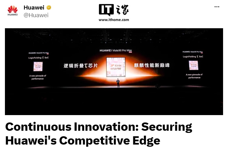
To circumvent limitations in accessing advanced manufacturing processes, Huawei is employing innovative strategies such as ‘Logic Folding’ to enhance chip capabilities. Yu explained that while high-end processors for smartphones necessitate advanced process nodes, many other components within a mobile device do not require such cutting-edge manufacturing. By adopting a holistic system engineering approach, Huawei aims to continuously optimize overall performance and compensate for the challenges associated with acquiring the most advanced fabrication technologies.
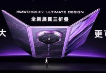
This strategy appears to be reflected in Huawei’s latest flagship smartphone series, the Mate 90 lineup, which was unveiled on October 1st. The entire series is powered by chips based on what Huawei calls the ‘Tao (τ) theory’. This theory introduces a new guiding principle for the evolution of semiconductors and electronic systems, shifting from ‘geometric scaling’ to ‘temporal scaling’ (τ scaling).
The Mate 90 series features different Kirin chip variants: the Kirin 9030 for the Mate 90 and the Kirin 9035 for the Mate 90 Pro. The more advanced Kirin 9050 and Kirin 9050 Pro chips are incorporated into the Mate 90 Pro Max and Mate 90 Pro Max / RS Ultimate Master models, respectively. These chips are said to leverage ‘Logic Folding’ and other innovations to improve performance.
Huawei’s official explanation of the Tao (τ) theory highlights that ‘Logic Folding’ and related core technologies form a multi-layered collaborative optimization system spanning devices, circuits, chips, and the overall system. The primary goal is to systematically reduce the time constant τ, thereby driving continuous improvements in performance, energy efficiency, and transistor density at all levels.
- Device Level: Optimizing transistors, interconnect resistance, and parasitic capacitance to minimize the device-level time constant τ at the physical layer.
- Circuit Level: Employing ‘Logic Folding’ to break through the physical limitations of traditional planar layouts. This significantly shortens critical path wiring lengths and reduces signal propagation resistance and capacitance loads, leading to substantial improvements in transistor density and circuit performance.
- Chip Level: Utilizing full-stack hardware-software-chip co-design principles. This approach enables fine-grained control of instruction and data flows based on actual workloads, enhancing system parallelism and efficiency, and drastically reducing end-to-end execution time.
- System Level: Defining flexible buses and reconstructing computing system interconnect protocols. This allows for unified memory addressing and native memory semantics for super nodes, greatly reducing system communication latency.
Looking ahead, Huawei anticipates that by 2031, high-end chips based on the Tao (τ) theory will achieve an equivalent transistor density comparable to 1.4nm process technology. This projection underscores Huawei’s commitment to pushing the boundaries of semiconductor innovation despite external challenges.